
SCACS: Atomic-to-Continuum Physics
Atomic-scale physics for confident pre-fabrication decisions on advanced semiconductor packages.LABLos Alamos National LabVERTICALAdvanced ManufacturingAI & AutonomySTAGE◆VENTURE BUILDTRL 4PISDr. Chinonso Ugwumadu, Dr. Roxanne TutchtonTear SheetNarrative
[]to switch
01
Overview
THE PROBLEM
Advanced packaging is the binding constraint on AI chip supply. TSMC’s CoWoS line (chip-on-wafer-on-substrate) is sold out through 2026 and scaling from roughly 35,000 to 130,000 wafers per month, yet packaging design teams are still losing months to prototype-test-fail cycles because the simulation tools they rely on cannot predict what will happen at the interfaces inside a modern 3D stack. A thermal interface material that simulates well as a bulk property fails in qualification because grain boundaries, voids, and atomic-scale disorder in the actual deposited film concentrate heat in ways the model never showed. The result is repeated fabrication runs, missed tape-out windows, and qualification delays that cost OSATs and IDMs tens of millions of dollars per failed package design.
THE BREAKTHROUGH
SCACS (Simulator Collection for Atomic-to-Continuum Scales) resolves the physics that existing simulation tools cannot: atomic-scale thermal and electronic transport at the interfaces inside advanced semiconductor packages. Where Ansys Icepak, Siemens Flotherm, and Cadence Celsius treat materials as bulk continua with uniform properties, SCACS uses machine-learned interatomic potentials trained on first-principles physics to generate build-relevant, stack-specific conductivity fields that reflect the actual deposited microstructure of a given TIM, underfill, solder alloy, or substrate dielectric. The output is not a generic improvement in simulation accuracy; it is a prediction tied to a specific material choice in a specific package design, giving the engineer confidence to commit to fabrication before cutting silicon. The two core models (SPTC-AI for thermal transport, SPEC-AI for electronic conductivity) have been trained and benchmarked against density-functional theory on silicon, with the benchmark manuscript accepted in Physical Review Materials.
THE OPPORTUNITY
Three concrete workflows illustrate where the value lands. TIM selection for CoWoS interposer stacks: a packaging engineer evaluating sintered silver versus epoxy-based TIMs for a specific die-to-interposer bond can run both material systems through SCACS and get stack-specific hotspot predictions before committing to a TIM supplier, cutting one or two prototype-fabrication cycles out of the qualification timeline. Underfill qualification for 3D IC: an OSAT qualifying a new capillary underfill for a high-bandwidth-memory stack can simulate the underfill’s thermal behavior at the actual fill geometry and void distribution rather than at bulk properties, reducing the risk of a late-stage thermal-cycling failure. Substrate dielectric screening: a supplier proposing a new low-k dielectric to an IDM can deliver simulation results the IDM’s thermal team can validate against fabrication data, shortening the supplier qualification cycle.
SCACS delivers its predictions through the finite-element solvers packaging teams already trust (Ansys, Abaqus, COMSOL, MOOSE), which eliminates adoption friction, but the product the customer is buying is the physics, not a plugin. The CAE market is $12.3B in 2025 growing to $20B by 2030 (MarketsandMarkets, 10.2% CAGR), with electronic thermal simulation a $2.3B sub-segment. SCACS targets the subset of that spend where interface-scale physics drives the production outcome.
ATOMIC-TO-CONTINUUM THERMAL SIMULATION
What continuum CAE blurs, SCACS resolves
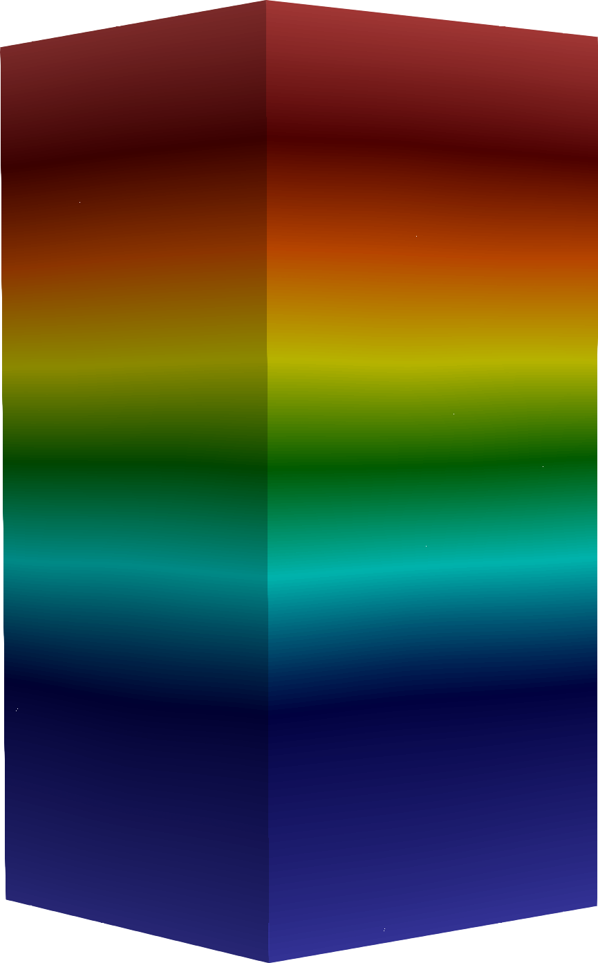
Conventional finite-element CAE homogenizes silicon into a smooth continuum. SCACS resolves the atomic lattice directly — so the heat-flux and temperature fields it computes keep structure the other tools average away.
CONVENTIONAL CAEContinuum finite-element mesh
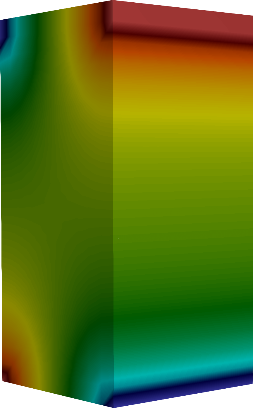

SCACSAtomic-to-continuum solver
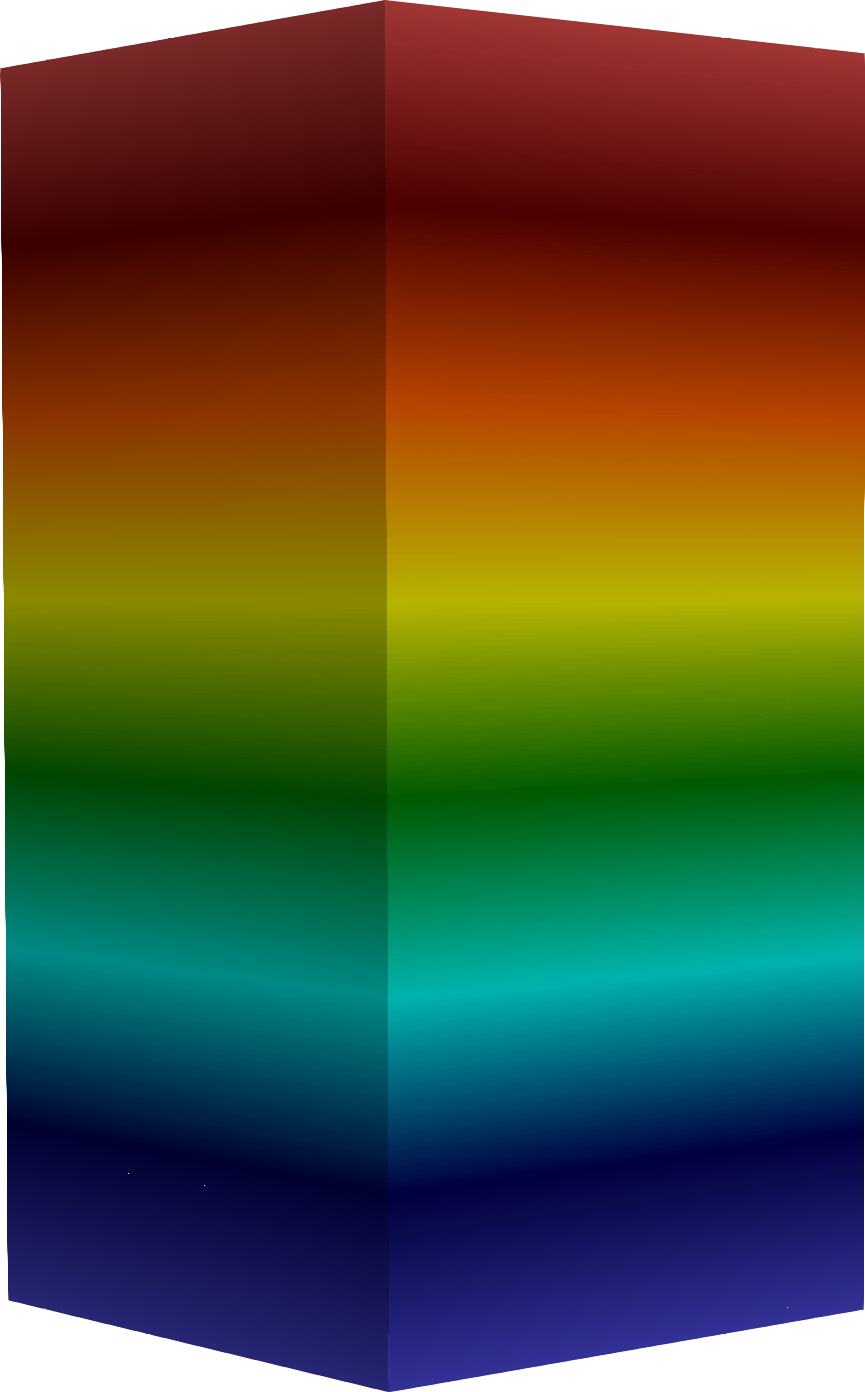
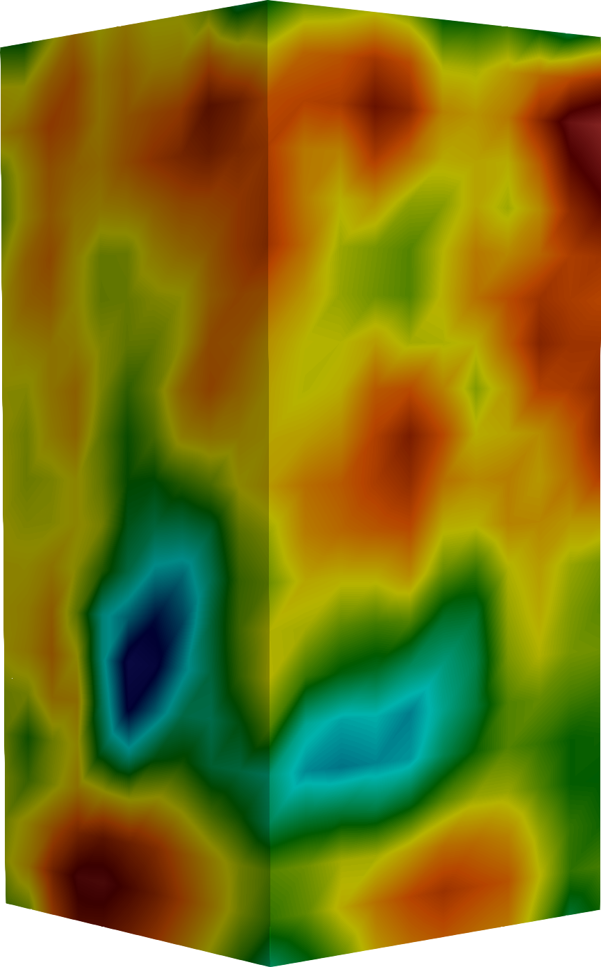
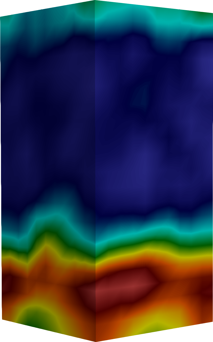
Continuum finite-element CAE (top) yields smoothly varying fields; SCACS (bottom) resolves atomic-scale thermal transport across the same silicon volume. Source renders: Los Alamos National Laboratory.
02
Key details
TECHNOLOGY STATUS
TRL 4. SPTC-AI (site-projected thermal conductivity) and SPEC-AI (site-projected electronic conductivity) models trained and benchmarked on silicon against density-functional theory. Silicon benchmark manuscript accepted in Physical Review Materials. Company reports 4x speedup over Abaqus on internal test cases (not independently validated). No production deployments and no paying customers yet. CRADA discussions in progress with CONSOL Innovations (West Virginia). Key next milestone: deliver a build-relevant prediction on a real packaging material system (TIM, underfill, or substrate dielectric) that a customer’s thermal team can validate against fabrication data.
IP POSITION
Provisional patent filed covering the site-projected conductivity models (SPTC-AI thermal and SPEC-AI electronic) and the workflow for coupling atomistic conductivity fields into commercial finite-element solvers. The IP covers the physics-trained machine-learning approach and the model-to-FE coupling, not the general concept of ML interatomic potentials (where MACE, NequIP, and Allegro are the academic state of the art).
DEPLOYMENT ARCHITECTURE
SCACS is not a standalone simulator. It delivers atomic-scale conductivity fields into the finite-element solvers customers already trust: Ansys, Abaqus, COMSOL, and MOOSE. The engineer does not change their workflow, their UI, or their procurement path; they get better physics inside the tool they already validate against. This is the adoption wedge, not the product. The product is the physics: build-relevant, stack-specific predictions for TIM, underfill, solder, and substrate dielectric systems that continuum solvers cannot resolve. Productization beyond the initial services engagement requires (1) packaging the models for customer use behind a stable API, (2) building the validation harness that proves predictions against fabrication data, and (3) hardening the FE-coupling layer for each target solver.
RESEARCH PROTOTYPE
The screens below are from the current SCACS research prototype — an early internal build the team uses to run the full atomistic-to-continuum workflow end to end, from mesh preparation through thermal solve to inspection. It is a working research tool for validating the physics on test cases, not the productized solver integration described above; the interface, packaging, and finite-element coupling layer are all still pre-production.
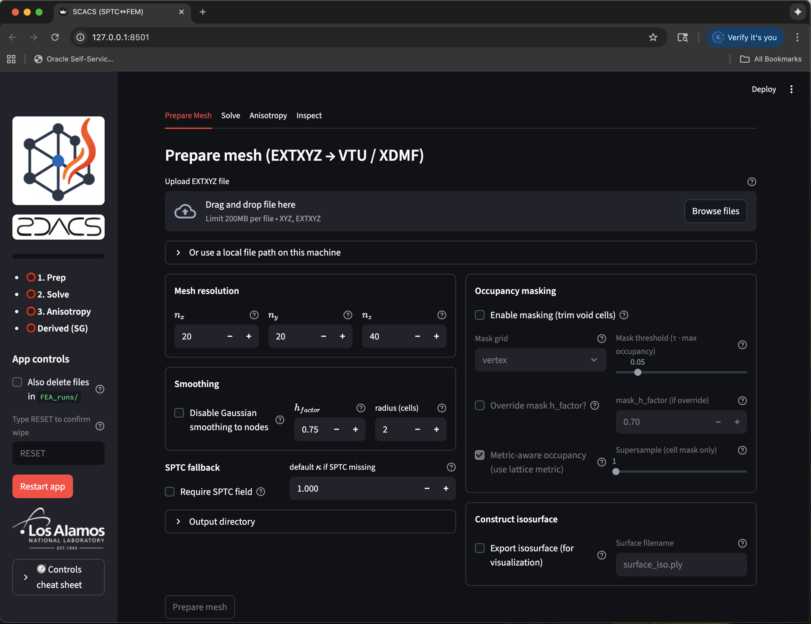
Prepare Mesh — the prototype converts an atomistic structure (EXTXYZ) into a finite-element mesh and applies SPTC-derived conductivity fields, with controls for mesh resolution, Gaussian smoothing, and occupancy masking. Early internal build.
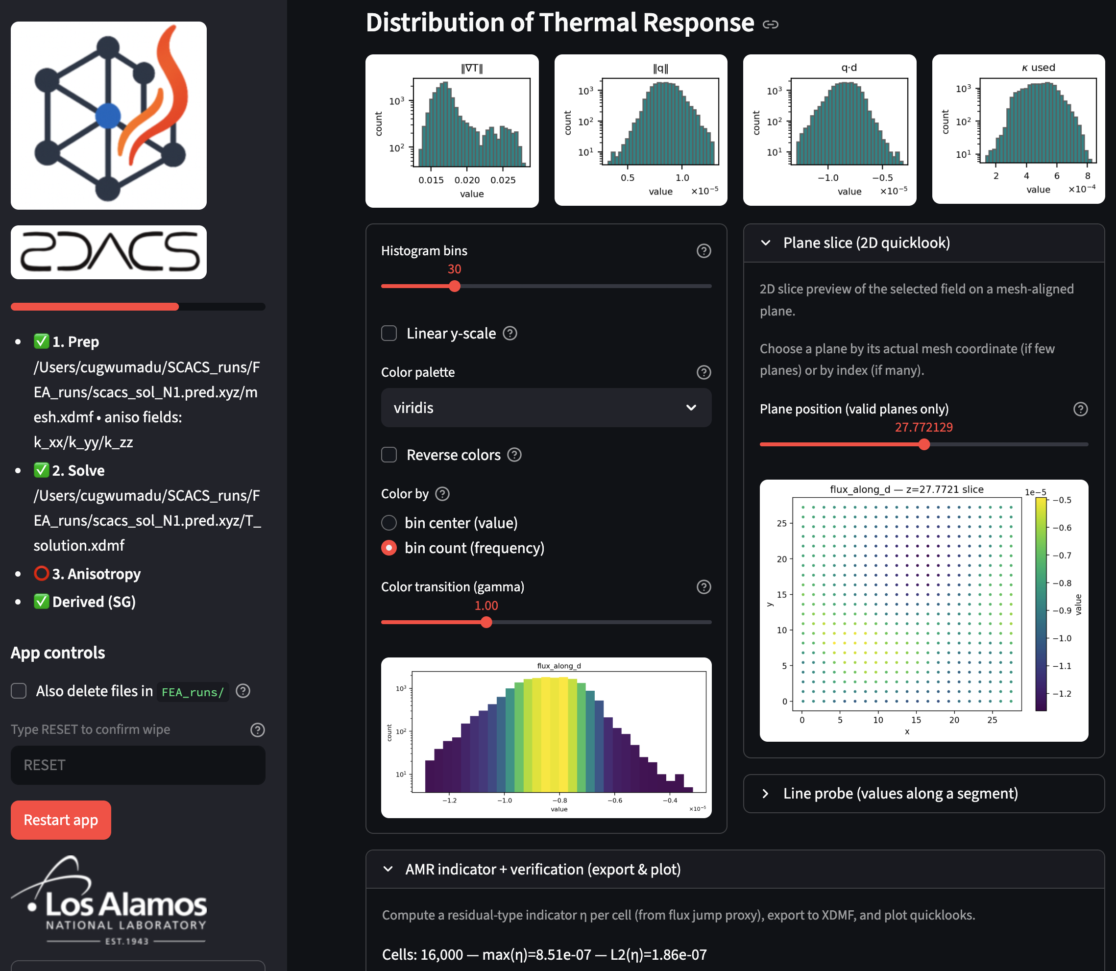
Inspect — distributions of temperature gradient, heat flux, and conductivity for a solved silicon test case, with a 2D plane-slice quicklook and a residual-based mesh-refinement (AMR) verification indicator.
MARKET OPPORTUNITY
Beachhead: advanced semiconductor packaging simulation, selling into engineering teams that make pre-fabrication material and geometry decisions on 3D packages. Two distinct buyer profiles: packaging material suppliers qualifying new TIMs, underfills, and dielectrics for delivery to OSATs and IDMs; and packaging design groups at OSATs and IDMs making die-to-substrate material decisions.
| SEGMENT | SIZE | TRAJECTORY |
|---|---|---|
| CAE market (full) | $12.3B (2025) | $20B by 2030, 10.2% CAGR |
| Electronic thermal simulation | $2.3B (2025) | $3.9B by 2031, 9.4% CAGR |
Buyers. OSATs (ASE, Amkor); TIM and substrate suppliers (Henkel, Shin-Etsu, Dow); IDM packaging groups (TSMC, Intel, Samsung, SK hynix). HBM, CoWoS, and 2 to 3 nm are the three named AI-supply bottlenecks, and the interface-physics regime SCACS resolves is exactly where those bottlenecks now sit.
Expansion. Once the packaging beachhead is proven, the same atomistic-to-continuum coupling extends to fusion plasma-facing components, spacecraft refractory materials, and biomedical device qualification as follow-on verticals where heterogeneous interface physics governs the production outcome.
03
Technical team & commercialization path
TECHNICAL TEAM
Tech Lead, Dr. Chinonso Ugwumadu.Postdoctoral Fellow, LANL T-4 Quantum and Condensed Matter Physics. Principal inventor of the site-projected conductivity models (SPTC-AI thermal, SPEC-AI electronic). Active participant in the UC/LANL Postdoc Entrepreneur Accelerator Program. LinkedIn
Co-Tech Lead, Dr. Roxanne Tutchton.Scientist, LANL T-4. Quantum and condensed matter physics; co-developer of the site-projected conductivity framework. LinkedIn
COMMERCIALIZATION PATH
Model, services-led year one. First-year engagements deliver a solved package problem (e.g., TIM selection validated against fabrication data), not a software license. Transition to licensed software with outcome-based pricing once a repeatable workflow is proven across two or three customers.
Beachhead customer, one named partner. One OSAT (ASE or Amkor) or one TIM/underfill supplier (Henkel, Shin-Etsu, or Dow) for a bounded package simulation problem where the pre-fabrication decision depends on interface-scale physics.
Adoption wedge, FE solvers. SCACS delivers its physics through the finite-element solvers customers already trust (Ansys, Abaqus, COMSOL, MOOSE). Engineers get better physics inside a familiar workflow, with no tool replacement, no new UI, and no procurement friction. The wedge is the workflow; the product is the physics.
Go-to-market, LANL-anchored with CHIPS R&D. LANL credibility alongside CHIPS R&D and Microelectronics Commons hub projects. Technical sell into packaging design and thermal engineering leaders.
Non-dilutive funding. DOE STTR/SBIR, CHIPS R&D packaging programs, Microelectronics Commons hubs, and NIST-affiliated advanced-packaging PMC activity extend runway while a commercial CEO is recruited.
04
Risks & mitigants
TECHNICAL · SILICON-TO-PACKAGING TRANSFER
SPTC-AI and SPEC-AI are benchmarked on silicon. Advanced packaging systems are mixed organic, ceramic, and metallic composites (solder resist, epoxy molding compound, sintered silver TIMs, low-k dielectrics) where the training data and underlying physics are different. Machine-learning interatomic potentials in the MACE and NequIP family have shown strong transferability at the research frontier, but generating build-relevant predictions for heterogeneous package stacks is unproven. Mitigant: phased model buildout by material class, anchored to a bounded customer package problem (e.g., a specific die-to-substrate TIM stack) rather than a general-purpose packaging potential. The first engagement is scoped to deliver a prediction the customer can validate against their own fabrication data.
MARKET · INCUMBENT AI-ACCELERATED THERMAL SIMULATION
Incumbents are investing in AI-accelerated thermal simulation. In November 2024, Ansys announced integration of NVIDIA Modulus into RedHawk-SC Electrothermal with a demonstrated 100x speedup. Siemens Flotherm’s BCI-ROM reduced-order models already deliver 40,000x speedup on pre-characterized systems. Both accelerate continuum physics; neither resolves atomic-scale transport at interfaces, which is where the failure modes in modern 3D packages now sit. Mitigant: SCACS competes on physics the incumbents do not have, not on speed or workflow. The value is demonstrated on packages whose qualification failures trace to interface-scale effects that Icepak, Flotherm, and Celsius cannot capture, with CHIPS R&D access securing the first design-tool engagements.
EXECUTION · NO COMMERCIAL TEAM, PROVISIONAL IP
The technology is strong but the commercial team is not yet in place, and with only a provisional patent filed the IP moat is still forming. Software ventures spun out of national labs historically under-index on commercial traction. Mitigant: pursue a services-led first engagement with one named OSAT or TIM supplier, scoped to a real package problem where fabrication data validates the prediction. Attach to CHIPS R&D and Microelectronics Commons non-dilutive funding to extend runway while a commercial CEO is recruited. CEO hire is gated to the first paying engagement, not to the seed close.
05
Competitive landscape
ANSYS ICEPAK + NVIDIA MODULUS · INCUMBENT, CONTINUUM CFD
Industry-standard electronic thermal CFD, now augmented with AI accelerators (100x speedup via the Ansys/NVIDIA partnership, November 2024, integrated with RedHawk-SC Electrothermal). Operates on continuum models with bulk material properties. The Modulus integration accelerates continuum physics; it does not add atomic-scale physics. SCACS addresses the regime Icepak cannot resolve, and delivers its predictions through Ansys workflows to eliminate adoption friction.
SIEMENS SIMCENTER FLOTHERM · INCUMBENT, CONTINUUM CFD
34 years in electronic cooling CFD. BCI-ROM compact models deliver up to 40,000x speedup on pre-characterized systems. Deep ecosystem and customer lock-in. Same limitation as Icepak: continuum-only, no atomic-scale physics. SCACS enters the same simulation segment with physics Flotherm does not have.
CADENCE CELSIUS & SYNOPSYS SENTAURUS · INCUMBENT, EDA-INTEGRATED
EDA-integrated electronic-thermal solvers that live inside existing chip design flows. Both are continuum solvers operating on bulk material properties. SCACS’s atomistic capability provides stack-specific predictions these tools cannot generate for modern 3D interface regimes.
MATLANTIS (PREFERRED NETWORKS) · ADJACENT, GENERAL-PURPOSE MLIP
The most commercially mature general-purpose ML interatomic potential. 100+ corporate customers; U.S. office opened 2025. Broad element coverage (72+) but no dedicated packaging-thermal workflow and no coupling to the continuum package simulators chip designers use. SCACS is narrower, deeper, and purpose-built for the packaging qualification problem.
ORBITAL MATERIALS & CITRINE INFORMATICS · ADJACENT, MATERIALS AI
Orbital raised $16M Series A in February 2024 (Radical Ventures, Toyota Ventures) on a foundation model targeting cleantech, not semiconductors. Citrine has raised roughly $76M on a data-driven materials informatics platform with no ab initio capability. Neither targets advanced-packaging simulation.
OPEN-SOURCE MLIPS · ADJACENT, ACADEMIC
MACE, Allegro, and NequIP are the state-of-the-art equivariant neural-network potentials from academic groups. MACE leads published benchmarks on thermal conductivity prediction. Free, powerful, and require significant ML-and-materials expertise to deploy, validate, and couple to industrial FE pipelines. SCACS’s thesis is that a packaging design group will buy physics that has been productized and calibrated on a specific package workload rather than a silicon benchmark.
SCACS is not a faster version of the continuum tools or a general-purpose atomistic platform. It is the tool that resolves the specific physics, atomic-scale thermal and electronic transport at heterogeneous interfaces, that now governs qualification outcomes for advanced 3D packages. The incumbents accelerate continuum models that smooth over interface effects; the general-purpose atomistic platforms have the physics but no packaging workflow. SCACS occupies the intersection: packaging-specific, interface-accurate, and delivered through the FE solvers that already own the engineering workflow.
06
What needs to happen next
- First customer-coupled materials model (priority). Deliver a build-relevant prediction on a real packaging material system (TIM, underfill, or substrate dielectric) that a customer’s thermal team can validate against fabrication data. This is the single most important commercial de-risk and the gate to the seed close.
- Beachhead customer commitment. Secure one named OSAT (ASE or Amkor) or one TIM/underfill supplier (Henkel, Shin-Etsu, or Dow) for a scoped package simulation engagement where the pre-fabrication decision depends on interface-scale physics.
- Commercial CEO recruitment. Identify and onboard an operator with semiconductor packaging or simulation-software experience.
- Exclusive license negotiation with LANL. Convert the provisional patent and pre-formation IP position into a license to the spinout vehicle.
- CRADA execution with CONSOL Innovations. Close the in-progress CRADA discussions and use the engagement as a validation pathway alongside the first commercial customer.
- Non-dilutive funding stack. File DOE STTR/SBIR; attach to CHIPS R&D packaging programs and Microelectronics Commons hub activity; pursue NIST-affiliated advanced-packaging PMC funding to extend runway.
- Productization roadmap. Define the path from one-off services engagement to a stable API and validation harness that allows licensing across two or three customers without bespoke model rebuilds per stack.
ON THIS PAGE
- Overview
- Key details
- Technical team & commercialization path
- Risks & mitigants
- Competitive landscape
- What needs to happen next
Read the long-form narrative→
DISCLAIMER
This analysis is provided for informational purposes only and does not constitute investment advice. Market estimates, technology assessments, and competitive analyses involve significant assumptions that may prove incorrect. Early-stage technologies carry substantial risk, including the possibility of total loss.
Narrative
LOS ALAMOS NATIONAL LABORATORY
The thermal wall inside every chip.
Advanced packaging has become the binding constraint on AI chip supply, and the interface layers inside a modern 3D package are now thin enough that atomic-scale physics governs how they perform. The simulation tools chip designers rely on today were built for bulk materials and cannot resolve that physics, leaving packaging engineers trapped in prototype-test-fail cycles that cost months and millions of dollars per failed design. A team at Los Alamos is building a multi-scale simulation platform that resolves the interface physics those tools cannot.
8 MIN READ
THE SHORT VERSION
Advanced packaging — not logic nodes — has become the binding constraint on AI chip supply, and the interface layers inside a modern 3D package are now thin enough that atomic-scale physics governs how they perform. The continuum simulation tools chip designers rely on assume bulk material properties and cannot resolve that physics, so a thermal interface material that simulates well still fails qualification, sending packaging teams back through fabrication cycles that cost months and millions. SCACS, built in Los Alamos National Laboratory’s T-4 Division, closes that gap: it couples machine-learning interatomic potentials trained on first-principles physics with site-projected conductivities — each atom’s contribution to bulk transport — to predict how the real deposited microstructure behaves. It delivers that physics through the continuum solvers packaging teams already trust (Ansys, Abaqus, COMSOL, MOOSE), so there is no tool replacement and no procurement friction. The buyers are concrete: the OSATs, substrate suppliers, and device makers making daily pre-fabrication decisions with tools that cannot see their failure mode.
Why heat has become the packaging problem
While the public narrative around AI compute focuses on leading-edge logic nodes, the binding supply constraint has shifted to advanced packaging. TSMC’s chief executive has told investors on successive earnings calls that the company’s CoWoS line, the chip-on-wafer-on-substrate process that bonds AI logic dies to high-bandwidth memory on a shared silicon interposer, is fully booked, and TSMC has committed to grow that line from roughly 35,000 wafers per month at the end of 2024 to roughly 130,000 per month by the end of 2026, a near-fourfold expansion that is already oversubscribed.1
Inside those packages, the governing constraint is heat. Modern AI accelerators stack logic dies vertically, bond them through interface layers a few microns thick, and push current through back-side power delivery networks, with every added interface contributing thermal resistance and every reduction in interconnect pitch making heat harder to move out. Junction temperatures now routinely approach the material limits of the solder, epoxy, and polymer underfills that surround them, materials that were never formulated for 500-watt dies stacked at sub-10 micron pitch.2
The industry’s response is to redesign the package itself, with new interface geometries, thinner underfills, tighter thermal paths, and new substrate stacks. The tools chip designers rely on to simulate those packages, Ansys Icepak, Siemens Simcenter Flotherm, and Cadence Celsius, were built around continuum thermal models that assume bulk material properties and smooth interfaces, yet the physics that now governs performance in a modern 3D package lives in the thin, disordered, atomic-scale interface layers that those continuum tools cannot resolve. A thermal interface material or underfill that simulates well as a bulk property fails in qualification because grain boundaries, voids, and atomic-scale disorder in the actual deposited film concentrate heat in ways the model never showed, sending packaging teams back through another fabrication cycle.
TSMC CoWoS Capacity Ramp
Monthly wafer-out capacity, TSMC advanced packaging, 2023–202735K70K105K140KSOLD OUT THROUGH END-2026~130K~4×capacity expansion,pre-absorbed by demand20232024202520262027eWAFERS / MONTHAdvanced packaging, not logic dies, is the AI-chip capacity lid. TSMC is scaling CoWoS wafer capacity roughly fourfold from 2023 to 2027, and that expansion is sold out through end-2026. Sources: TSMC capacity disclosures and TrendForce industry reporting, 2024 to 2025.
The physics gap the continuum tools cannot close
Package simulation has been constrained for decades by the trade-off between physical accuracy and computational scale. First-principles atomistic calculations, the density functional theory that accurately predicts thermal and electronic transport at the atomic scale, cost days of supercomputer time per system and reach only a few hundred atoms, while classical molecular dynamics reaches device-relevant length scales only by relying on empirical interatomic potentials that break down the moment a new element, defect, or interface is introduced. The maturation of general-purpose machine-learning interatomic potentials over the last eight years has begun to collapse that trade-off, with platforms like Preferred Networks’ Matlantis now serving more than 100 corporate customers and academic models such as MACE leading published benchmarks on thermal conductivity prediction.3 None of those platforms has been coupled to the continuum package simulators chip designers actually use.
SCACS (Simulator Collection for Atomic-to-Continuum Scales) resolves the atomic-scale thermal and electronic transport physics that governs performance at the interfaces inside a modern 3D package. The tool couples machine-learning interatomic potentials trained on first-principles physics with what the team calls site-projected conductivities: the contribution of each atom in a structure to the bulk thermal or electronic transport property. Instead of assuming a single bulk value for a given material, the simulation produces build-relevant, stack-specific conductivity fields that reflect the actual deposited microstructure. That output feeds into SCACS’s built-in continuum solver or the commercial solver the team already trusts, so the simulation finally captures what happens at the interfaces that continuum tools smooth over, and the engineer gets a prediction tied to the specific material choice in the specific package design being qualified.
Length Scale Versus Physical Accuracy
Where each simulation class sits — and the gap SCACS bridgesSCACSatomic-to-continuum bridgeDFT~10² atomsML-IPsMACE · NequIPClassical MDempirical potentialsContinuum FEAnsys · CadenceÅnm10 nmµm10 µmmmLENGTH SCALE (log)first-principles accuracybulk-propertyPHYSICAL ACCURACYEvery simulation class trades physical accuracy against the length scale it can reach. First-principles DFT is near-exact but limited to a few hundred atoms; continuum finite-element tools span an entire package but assume bulk material properties. Machine-learned interatomic potentials collapse that trade-off, and SCACS is the bridge that carries their atomic-scale accuracy into the finite-element workflow packaging teams already use.
SCACS delivers its physics through the continuum solvers packaging teams already trust (Ansys, Abaqus, COMSOL, MOOSE), which means no tool replacement and no procurement friction; the engineer’s workflow stays the same, and the physics input gets better. Three concrete use cases illustrate the fit. A packaging engineer evaluating sintered silver versus epoxy-based TIMs for a specific CoWoS die-to-interposer bond runs both material systems through SCACS, gets stack-specific hotspot predictions before committing to a supplier, and cuts one or two prototype-fabrication cycles out of the qualification timeline. An OSAT qualifying a new capillary underfill for a high-bandwidth-memory stack simulates the underfill’s thermal behavior at the actual fill geometry and void distribution rather than at bulk properties, reducing the risk of a late-stage thermal-cycling failure. A supplier proposing a new low-k dielectric to an IDM delivers simulation results the IDM’s own thermal team can reproduce inside their existing workflow, shortening the supplier-qualification cycle. In each case the value is a confident pre-fabrication decision, not a more accurate number in the abstract.
The approach draws on a specific scientific lineage. LANL’s T-4 Division has been running first-principles simulations of disordered and defect-rich materials for more than three decades, with an active body of work on amorphous systems, alloy phase stability, and radiation-damage chemistry that continues to shape the group’s computational expertise today.4 The reason this opportunity exists now rather than three years ago is that the methods and the problem have arrived in the same window: equivariant graph neural network potentials matured between 2022 and 2025, progressing from NequIP through MACE to r2SCAN-trained universal potentials, while CoWoS moved from a research curiosity to the binding supply constraint for AI compute.
The simulation segment the incumbents cannot serve
Commercial gravity follows the capital expenditure, and advanced packaging is now where both the industry’s capital and its binding physical constraints sit. TSMC has publicly committed to tens of billions of dollars of capacity expansion through 2026, with CoWoS and 2 to 3 nanometer logic absorbing most of the spend, and Samsung, SK hynix, Intel, and the OSAT suppliers (ASE, Amkor) have announced similarly large expansions.5 Inside those capital programs sit hundreds of millions of dollars of annual spend on thermal interface materials, underfills, low-k dielectrics, and substrate chemistries that the industry is actively working to improve.
The buyers are concrete: the packaging design and thermal engineering teams at the OSATs, substrate suppliers, and integrated device makers who are making daily pre-fabrication decisions with simulation tools that cannot resolve the physics driving their qualification failures. OSATs like ASE and Amkor are pushing die-to-substrate power densities above 2 watts per square millimeter and need confidence that a specific interface and underfill choice will survive thermal cycling before they commit to a production run, because each failed qualification cycle costs weeks of fab time and tens of millions of dollars. Substrate suppliers including Shin-Etsu, Dow, Henkel, and Kyocera are proposing new dielectric and substrate formulations to IDMs and need simulation results their customers’ thermal teams can validate, not bulk-property approximations the IDM has to re-test. IDM packaging design groupsat TSMC, Intel, Samsung, and SK hynix are architecting 3D stacks with layer thicknesses approaching the atomic scale and are looking for tools that reduce design iterations and accelerate qualification.
CAE Market and Electronic Thermal Sub-Segment
Nested market sizing — CAE down to the interface-scale beachheadCAE MARKET$12.3B → $20.0B10.2% CAGR · 2025–2030incumbents own the bulk-property segmentELECTRONIC THERMAL SIMULATION$2.3B → $3.9B9.4% CAGRSCACS BEACHHEADadvanced-packaging interface-scale simulationinterface-scale segment — unownedThe computer-aided engineering market is projected to reach $20B by 2030 at a 10.2% CAGR, with electronic thermal simulation a $2.3B sub-segment growing at 9.4%. SCACS targets the subset of that spend where interface-scale physics drives the production outcome. Source: MarketsandMarkets CAE Market Report, 2025.
Adjacent markets already show that enterprises will pay for physics-aware AI platforms. Matlantis has grown to more than 100 corporate customers in five years, Orbital Materials raised a $16 million Series A in early 2024 on a foundation model for materials discovery, and Citrine Informatics has raised roughly $76 million on a data-driven materials informatics platform.6 None of those platforms has been coupled to the continuum package simulators chip designers actually use, and none has chosen advanced packaging as a primary vertical, leaving the specific combination of atomistic accuracy, packaging design focus, and finite-element delivery unoccupied by a commercial product today.
Built at Los Alamos
SCACS originates in Los Alamos National Laboratory’s T-4 Division, the Quantum and Condensed Matter Physics group. T-4 has run first-principles materials simulations for more than thirty years, with a particular line of work on amorphous systems, disordered alloys, and defect chemistry in functional materials. The group has standing access to LANL’s high-performance computing infrastructure, its atomistic simulation expertise, and its position inside the Department of Energy’s CHIPS R&D and Microelectronics Commonsprograms.7
PRINCIPAL INVESTIGATOR
Dr. Chinonso Ugwumadu
LANL T-4 Quantum and Condensed Matter Physics. Atomistic simulation and machine-learning interatomic potentials. Principal inventor of the site-projected conductivity models underlying SCACS.
CO-TECH LEAD
Dr. Roxanne Tutchton
Scientist, LANL T-4. Quantum and condensed matter physics; co-developer of the site-projected conductivity framework.
SCACS turns atomic-scale physics into fewer design iterations, faster qualification, and confident production commitments for the packages the semiconductor industry is building now.
NOTES
- TSMC earnings call transcripts, Q3 2024 and Q4 2024; TrendForce advanced packaging capacity analysis, January 2025. ↩
- ITRS/IEEE advanced packaging thermal roadmap; junction temperature constraints documented in JEDEC JEP158 and related industry specifications. ↩
- Batatia et al., “MACE: Higher Order Equivariant Message Passing Neural Networks for Fast and Accurate Force Fields,” NeurIPS 2022; Preferred Networks Matlantis corporate disclosures, 2025. ↩
- LANL T-4 Division publication record; Ugwumadu et al., accepted manuscript, Physical Review Materials, 2025. ↩
- TSMC, Samsung, Intel, and ASE capital expenditure disclosures, FY2024 to FY2025 earnings releases. ↩
- Orbital Materials Series A: Radical Ventures, Toyota Ventures, February 2024. Citrine Informatics: Crunchbase funding history, cumulative ~$76M through 2024. ↩
- DOE CHIPS R&D program and Microelectronics Commons hub program structure documentation, 2024. ↩
ON THIS PAGE
- Why heat has become the packaging problem
- The physics gap the continuum tools cannot close
- The simulation segment the incumbents cannot serve
- Built at Los Alamos
DISCLAIMER
This analysis is provided for informational purposes only and does not con

